|
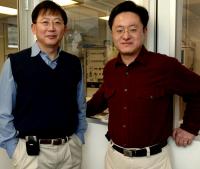
Princeton nanotechnologist Stephen Chou (left) with
graduate student Xiaogan Liang, the developers of a practical
technique for harnessing the power of carbon for more powerful
electronics.
Photo by Frank Wojciechowski
|
Until now, however, switching from silicon to
carbon has not been possible because technologists believed they
needed graphene material in the same form as the silicon used to make
chips: a single crystal of material eight or 12-inches wide. The
largest single-crystal graphene sheets made to date have been no wider
than a couple millimeters, not big enough for a single chip. Chou and
researchers in his lab realized that a big graphene wafer is not
necessary, as long they could place small crystals of graphene only in
the active areas of the chip. They developed a novel method to achieve
this goal and demonstrated it by making high-performance working
graphene transistors.
�Our approach is to completely abandon the classical methods that
industry has been using for silicon integrated circuits,� Chou said.
Chou, along with graduate student Xiaogan Liang and materials engineer
Zengli Fu, published their findings in the December 2007 issue of Nano
Letters, a leading journal in the field. The research was funded in
part by the Office of Naval Research.
In their new method, the researchers make a special stamp consisting
of an array of tiny flat-topped pillars, each one-tenth of a
millimeter wide. They press the pillars against a block of graphite
(pure carbon), cutting thin carbon sheets, which stick to the pillars.
The stamp is then removed, peeling away a few atomic layers of
graphene. Finally, the stamp is aligned with and pressed against a
larger wafer, leaving the patches of graphene precisely where
transistors will be built.
The technique is like printing, Chou said. By repeating the process
and using variously shaped stamps (the researchers also made strips
instead of round pillars), all the active areas for transistors are
covered with single crystals of graphene.
�Previously, scientists have been able to peel graphene sheets from
graphite blocks, but they had no control over the size and location of
the pieces when placing them on a surface,� Chou said.
One innovation that made the technique possible was to coat the stamp
with a special material that sticks to carbon when it is cold and
releases when it is warm, allowing the same stamp to pick up and
release the graphene.
Chou�s lab took the next step and built transistors - tiny on-off
switches - on their printed graphene crystals. Their transistors
displayed high performance; they were more than 10 times faster than
silicon transistors in moving "electronic holes" - a key measure of
speed.
The new technology could find almost immediate use in radio
electronics, such as cell phones and other wireless devices that
require high power output, Chou said. Depending on the level of
interest from industry, the technique could be applied to wireless
communication devices within a few years, Chou predicted.
�What we have done is shown that this approach is possible; the next
step is to scale it up,� Chou said.
|