|
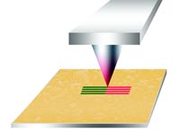
An animated look (SWF format) at how thermochemical
nanolithography works:
SWF = 2.84 MB [� Georgia Tech]
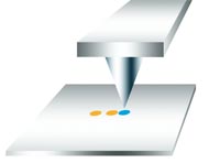
An animated look at how DPN works (not to scale):
SWF = 2.17 MB [� Georgia Tech]
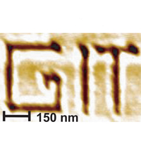
The initials for the Georgia Institute of Technology written with
the thermochemical nanolithography technique. (Image � Georgia
Tech)
|
The technique is surprisingly simple. Using an atomic force microscope
(AFM), researchers heat a silicon tip and run it over a thin polymer
film. The heat from the tip induces a chemical reaction at the surface
of the film. This reaction changes the film�s chemical reactivity and
transforms it from a hydrophobic substance to a hydrophilic one that
can stick to other molecules. The technique is extremely fast and can
write at speeds faster than millimeters per second. That�s orders of
magnitude faster than the widely used dip-pen nanolithography (DPN),
which routinely clocks at a speed of 0.0001 millimeters per second.
Using the new technique, researchers were able to pattern with
dimensions down to 12 nanometers in width in a variety of environments.
Other techniques typically require the addition of other chemicals to
be transferred to the surface or the presence of strong electric
fields. TCNL doesn�t have these requirements and can be used in humid
environments outside a vacuum. By using an array of AFM tips developed
by IBM, TCNL also has the potential to be massively scalable, allowing
users to independently draw features with thousands of tips at a time
rather than just one.
�Thermochemical nanolithography is a rapid and versatile technique
that puts us much closer to achieving the speeds required for
commercial applications,� said Elisa Riedo, assistant professor in
Georgia Tech�s School of Physics. �Because we�re not transferring any
materials from the AFM tip to the polymer surface (we are only heating
it to change its chemical structure) this method can be intrinsically
faster than other techniques.�
It�s the heated AFM tips that are one key to the new technique.
Designed and fabricated by a group led by William King at the
University of Illinois, the tips can reach temperatures hotter than
1,000 degrees Celsius. They can also be repeatedly heated and cooled 1
million times per second.
�The heated tip is the world�s smallest controllable heat source,�
said King.
TCNL is also tunable. By varying the amount of heat, the speed and the
distance of the tip to the polymer, researchers can introduce
topographical changes or modulate the range of chemical changes
produced in the material.
�By changing the chemistry of the polymer, we�ve shown that we can
selectively attach new substances, like metal ions or dyes to the
patterned regions of the film in order to greatly increase the
technique�s functionality,� said Seth Marder, professor in Tech�s
School of Chemistry and Biochemistry and director of the Center for
Organic Photonics and Electronics. Marder�s group developed the
thermally switchable polymers used in this study.
�We expect thermochemical nanolithography to be widely adopted because
it�s conceptually simple and can be broadly applied,� said Marder.
�The scope is limited only by one�s imagination to develop new
chemistries and applications.�
For nanolithography to be commercially viable, it must be able to
write at high speeds, be used in a variety of environments and write
on a variety of materials. While the technique demonstrated here
doesn�t yet allow writing at the centimeters per second rate that
would be ideal, it does put researchers much closer to the goal than
previous techniques. Once perfected, nanolithography could be used to
draw nanocircuits for the electronics industry, create nanochannels
for nanofluidics devices or be adapted for drug delivery or biosensing
technologies.
The research was supported by the National Science Foundation�s Center
for Materials and Devices for Information Technology Research, the
U.S. Department of Energy, the National Science Foundation, the
Georgia Institute of Technology Research Foundation, the GT College of
Sciences Cutting Edge Research Award and ONR Nanoelectronics. In
addition to Riedo, Marder and King, the interdisciplinary research
team consisted of Robert Szoszkiewicz, Takashi Okada, Simon Jones and
Tai-De Li from Georgia Tech.
|