Novel gate dielectric materials: perfection is not enough
For the first time theoretical modeling has provided a glimpse into how
promising dielectric materials are able to trap charges, something which
may affect the performance of advanced electronic devices. This is
revealed in a paper published on the 12th October in Physical Review
Letters by researchers at the London Centre for Nanotechnology and
SEMATECH, a company in Austin, Texas.
Through the constant quest for miniaturization, transistors and all
their components continue to decrease in size. A similar reduction has
resulted in the thickness of a component material known as the gate
dielectric � typically a thin layer of silicon dioxide, which has now
been in use for decades. Unfortunately, as the thickness of the gate
dielectric decreases, silicon dioxide begins to leak current, leading
to unwieldy power consumption and reduced reliability. Scientists hope
that this material can be replaced with others, known as
high-dielectric constant (or high-k) dielectrics, which mitigate the
leakage effects at these tiny scales.
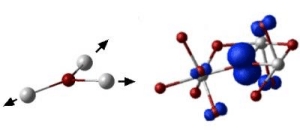
On the left is an Illustration of the displacement
of hafnium atoms (white) in the structure of hafnium oxide to
accommodate the presence of the self-trapped hole in the oxygen
atom (red). On the right is the quantum mechanics view of the
probability of finding a hole near certain atoms (larger blue
structures represent higher probability).
Image � by London Centre for Nanotechnology
Metal oxides with high-k have attracted
tremendous interest due to their application as novel materials in the
latest generation of devices. The impetus for their practical
introduction would be further helped if their ability to capture and
trap charges and subsequent impact on instability of device
performance was better understood. It has long been believed that
these charge-trapping properties originate from structural
imperfections in materials themselves. However, as is theoretically
demonstrated in this publication, even if the structure of the high k
dielectric material is perfect, the charges (either electrons or the
absence of electrons � known as holes) may experience �self trapping�.
They do so by forming polarons � a polarizing interaction of an
electron or hole with the perfect surrounding lattice. Professor
Alexander Shluger of the London Centre for Nanotechnology and the
Department of Physics & Astronomy at UCL says: �This creates an energy
well which traps the charge, just like a deformation of a thin rubber
film traps a billiard ball.�
The resulting prediction is that at low temperatures electrons and
holes in these materials can move by hopping between trapping sites
rather than propagating more conventionally as a wave. This can have
important practical implications for the materials� electrical
properties. In summary, this new understanding of the polaron
formation properties of the transition metal oxides may open the way
to suppressing undesirable characteristics in these materials.
The London
Centre for Nanotechnology is a joint enterprise between
University College London and Imperial College London. In bringing
together world-class infrastructure and leading nanotechnology
research activities, the Centre aims to attain the critical mass to
compete with the best facilities abroad. Furthermore by acting as a
bridge between the biomedical, physical, chemical and engineering
sciences the Centre will cross the 'chip-to-cell interface' - an
essential step if the UK is to remain internationally competitive in
biotechnology.
-
Source:
University College
London: Founded in 1826, UCL was the
first English university established after Oxford and Cambridge, the
first to admit students regardless of race, class, religion or
gender, and the first to provide systematic teaching of law,
architecture and medicine. In the government�s most recent Research
Assessment Exercise, 59 UCL departments achieved top ratings of 5*
and 5, indicating research quality of international excellence.